
Wirebond Packaging
Reliable, cost-effective interconnects trusted in high-volume manufacturing
Wirebond Packaging
Reliable, cost-effective interconnects trusted in high-volume manufacturing
Flip Chip Packaging
High-density, high-performance interconnects for advanced miniaturization
Flip Chip Packaging
High-density, high-performance interconnects for advanced miniaturization

Wafer Bumping
Foundational process technology for high-yield advanced packaging
Wafer Bumping
Foundational process technology for high-yield advanced packaging
Wafer Level Packaging
Advanced performance in ultra-compact form factors.
Wafer Level Packaging
Advanced performance in ultra-compact form factors.

System-in-Package
High-density integration without trade-offs in performance or footprint
System-in-Package
High-density integration without trade-offs in performance or footprint
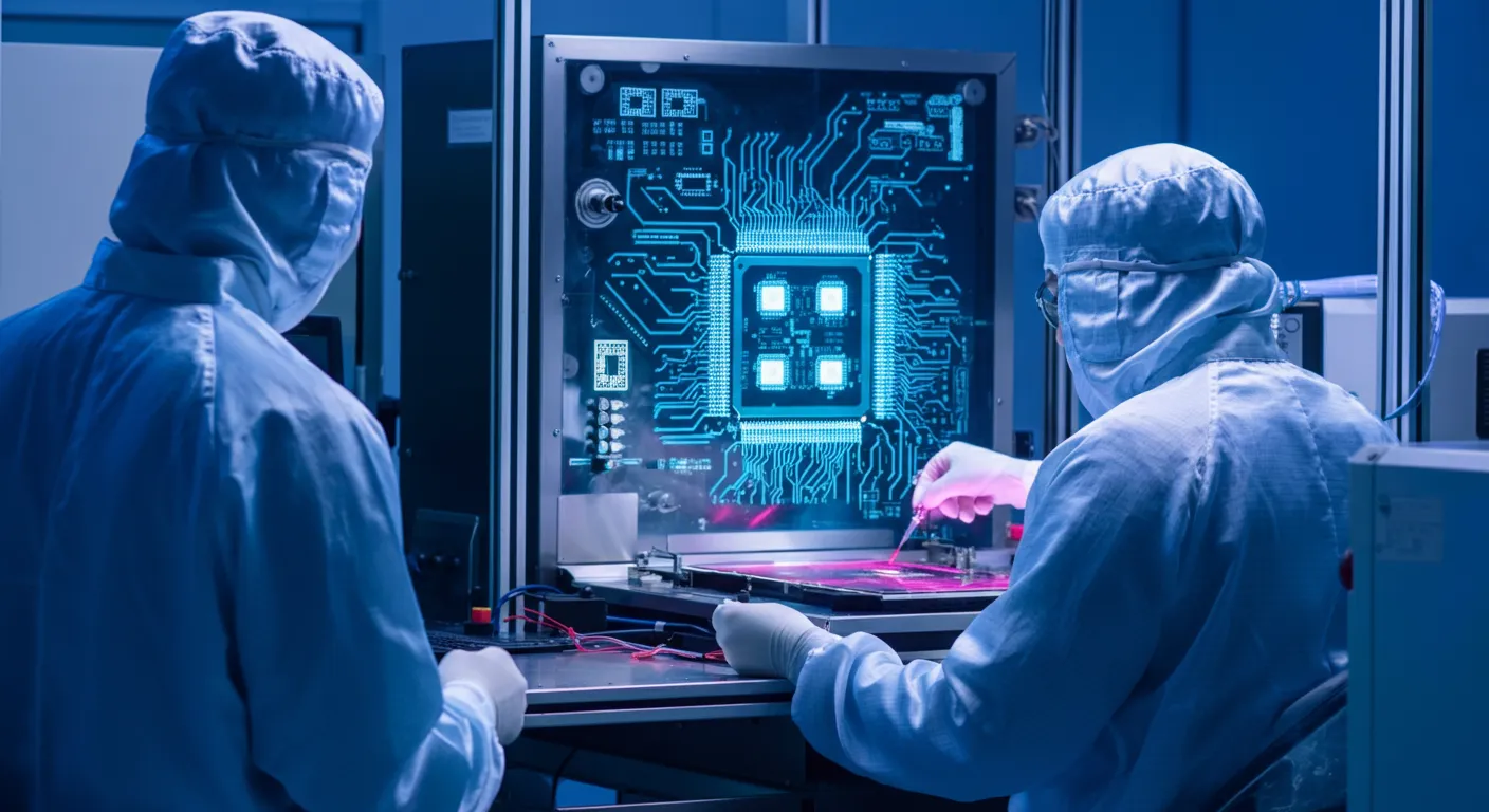
Wirebond Packaging
technology-wirebond-packaging
Wirebonding remains one of the most widely adopted methods in semiconductor assembly, connecting chips to substrates, substrates to substrates, or substrates to packages. We offer a full range of wirebond solutions across QFN, DFN, QFP, WB-BGA, and WB-LGA formats — with materials including gold, copper, silver, and palladium-coated wire. Backed by high-volume manufacturing and billions of units shipped, our platforms serve power, memory, MEMS, mobile, automotive, and beyond.
Flip Chip Packaging
flip-chip-packaging
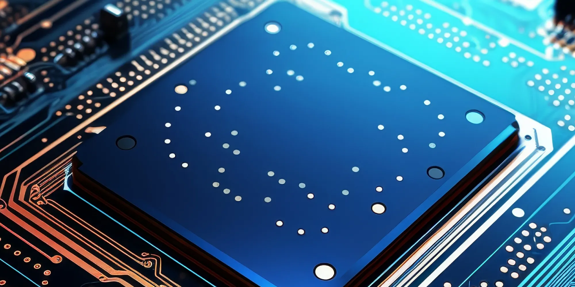
Flip chip technology enables direct die-to-substrate connections through solder bumps — reducing parasitics, improving thermal efficiency, and shrinking form factors.
We support a broad range of flip chip formats including fcCSP, fcBGA, C2W, and 3DIC. Applications span from large single-die packages with thermal enhancements to compact modules and AiP designs with embedded antennas.
Wafer Bumping
wafer-bumping
Wafer bumping enables high-density interconnects directly at the wafer level. It supports improved electrical performance, tighter form factors, and lower overall cost.
We provide bumping and redistribution services for 200mm and 300mm wafers, including redistribution and full turnkey support for flip chip and wafer-level packaging. Our process capabilities span printed bump, ball drop, and plated bumping with lead-free and copper pillar alloys—optimized for reliability and production scale.
Wafer Level Packaging
wafer-level-packaging
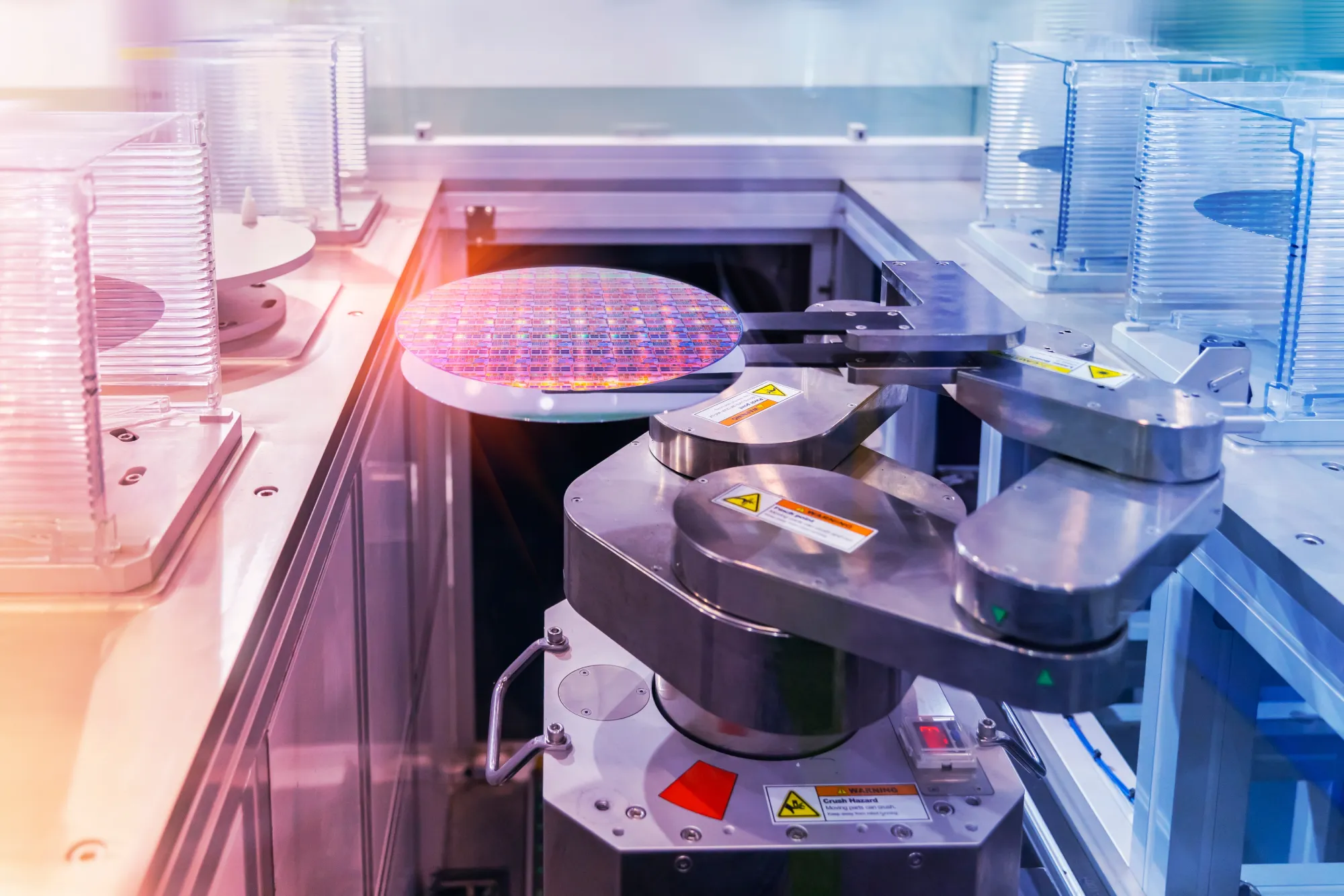
Wafer-level packaging integrates more functionality directly at the wafer stage, reducing size and improving power, speed, and signal integrity. It’s key to enabling next-gen devices that demand performance without compromising footprint or cost.
System-in-Package
system-in-package
System-in-Package (SiP) combines multiple chips and components into a single compact module, enabling faster processing, higher performance, and more functionality in less space.
Our platforms support heterogeneous integration of logic, analog, power, and memory ICs using SMT, wirebond, and flip chip. Advanced technologies include:
- Dual-sided molding – reduces package size, shortens routing, lowers resistance, and improves system performance
- EMI shielding – enhances thermal conductivity and signal integrity via backside metallization
- Laser-assisted bonding (LAB) – overcomes traditional reflow issues like warpage, stress, and CTE mismatch for improved reliability
MEMS & Sensors Packaging
mems-sensors-packaging
MEMS and sensor packaging enables real-time sensing, responsiveness, and control in compact, power-efficient designs. These technologies are foundational across communications, automotive, medical, industrial, and consumer systems.
Our dedicated MEMS team supports full turnkey development including packaging co-design, simulation, BOM qualification, assembly, testing, and quality assurance. We deliver highly integrated, size-optimized solutions that meet the performance and cost demands of modern sensing applications.
2.5/3D Packaging
2-5-3d-packaging
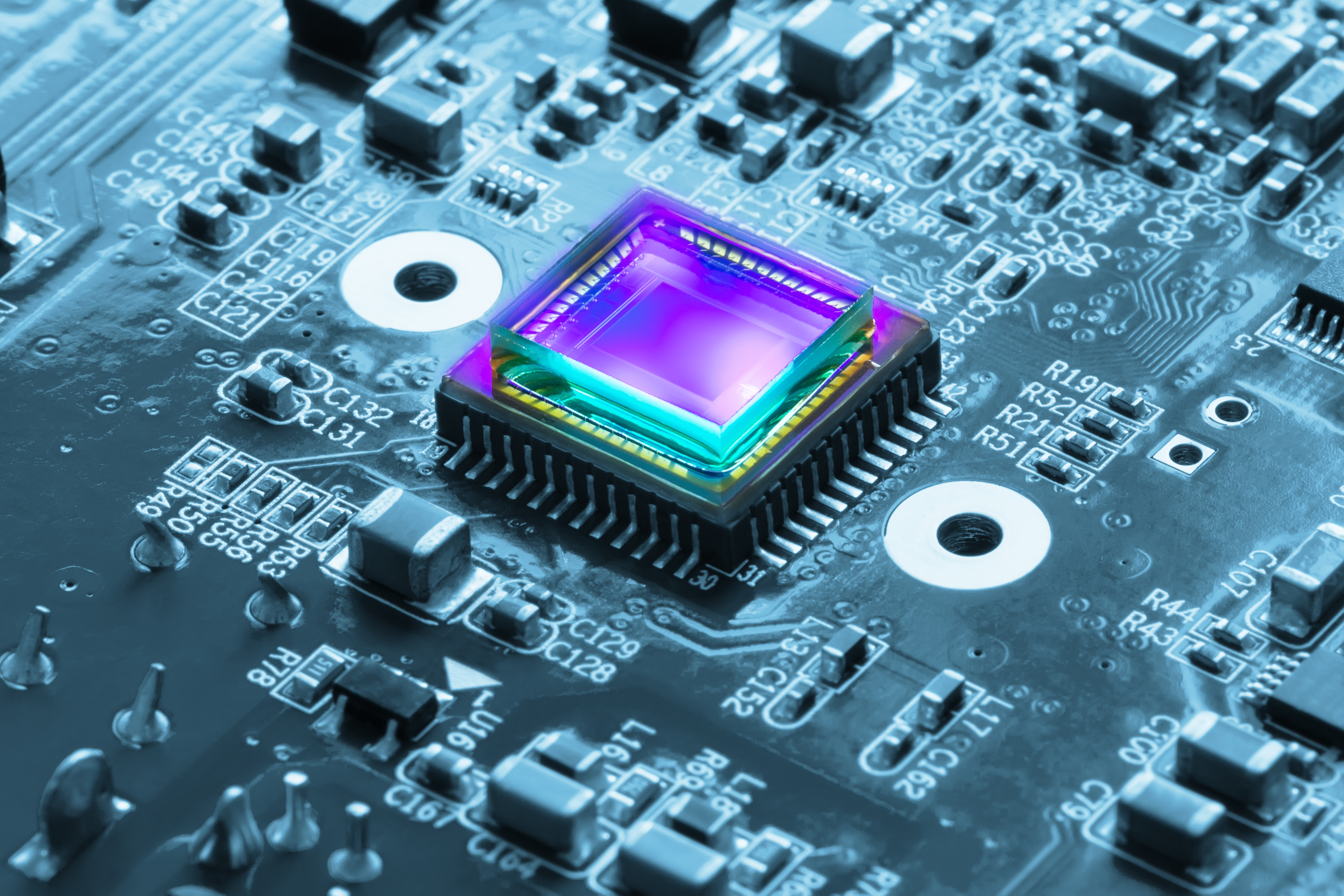
Advanced 2.5D and 3D packaging stacks and interconnects multiple components to maximize functionality and performance.